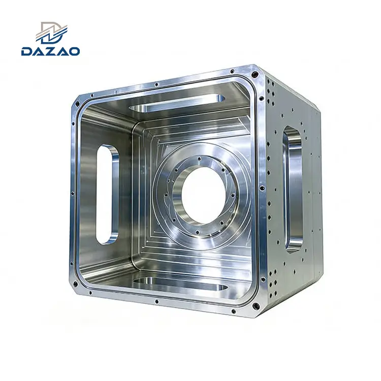
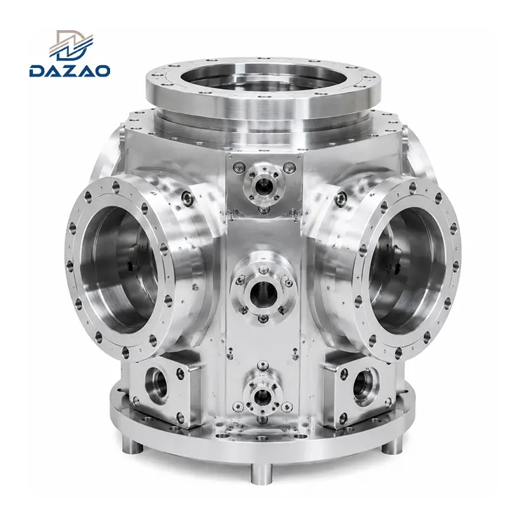
5 Axis CNC Machining Semiconductor Vacuum Chamber Engineering Specifications
Monolithic milled vacuum enclosures engineered for zero-defect vacuum integrity, low outgassing, and long-term dimensional stability.
Core Engineering Features:
Helium leak rate ≤1×10^-12 Pa·m³/s with 100% test reports.
Austenitic stainless steel 304/316L and 6061-T6 aluminum alloys.
Ultra high vacuum chamber fabrication down to 10^-9 Pa.
Flange sealing surface flatness tolerance held within ≤0.02 mm/m.
Semiconductor load lock chamber design with stress relief.
15-day prototype turnaround for engineering evaluation models.
Zeiss CMM validated high precision cnc machining semiconductor parts.
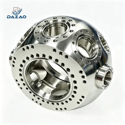
Monoblock Milling Capabilities for Semiconductor Vacuum Chambers
Eliminating structural welds to achieve helium-tight seals and superior mechanical integrity in process chambers.
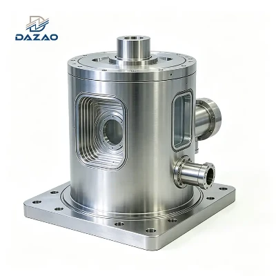
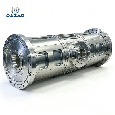
Xiamen Dazao Machinery produces monoblock 5-axis CNC machined semiconductor vacuum chambers designed for high vacuum (HV) and ultra-high vacuum (UHV) systems. Utilizing multi-axis turning and 5-axis simultaneous CNC milling centers, solid billets of stainless steel 304, 316L, and Al6061-T6 are converted into precise vacuum enclosures without structural welds.
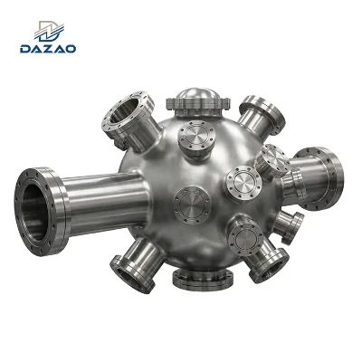
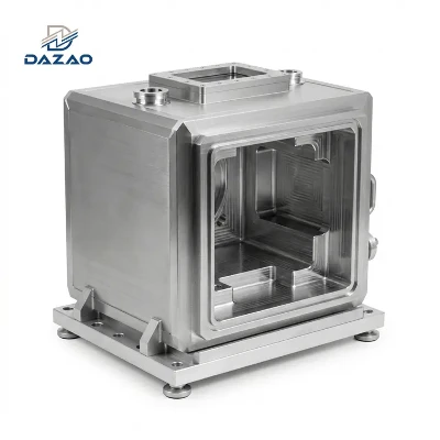
Our production capabilities support box-shaped PVD deposition chambers, plasma etching chambers, wafer load lock modules, and spherical UHV reaction vessels. By eliminating internal porosity, material voids, and heat-affected zone weld defects, our 5 Axis CNC Machining Semiconductor Vacuum Chamber process delivers stable sealing boundaries, continuous internal cooling channels, and distortion-free flange faces for global toolmakers.
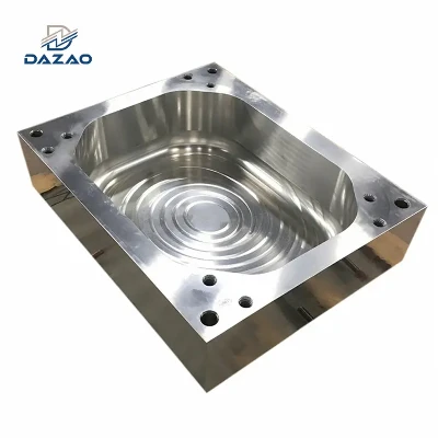
Field Failure Analysis and Engineering Corrective Actions
Real-world engineering root cause reviews from semiconductor equipment field installations.
1: PVD Deposition Chamber Flange Micro-Leakage Rectification
· Root Cause: A European thin-film equipment client experienced a 30% failure rate during helium leak testing on box-shaped stainless steel PVD chambers machined by a legacy vendor. Failure analysis revealed microscopic feed marks and a flange flatness deviation exceeding 0.05 mm across the sealing face.
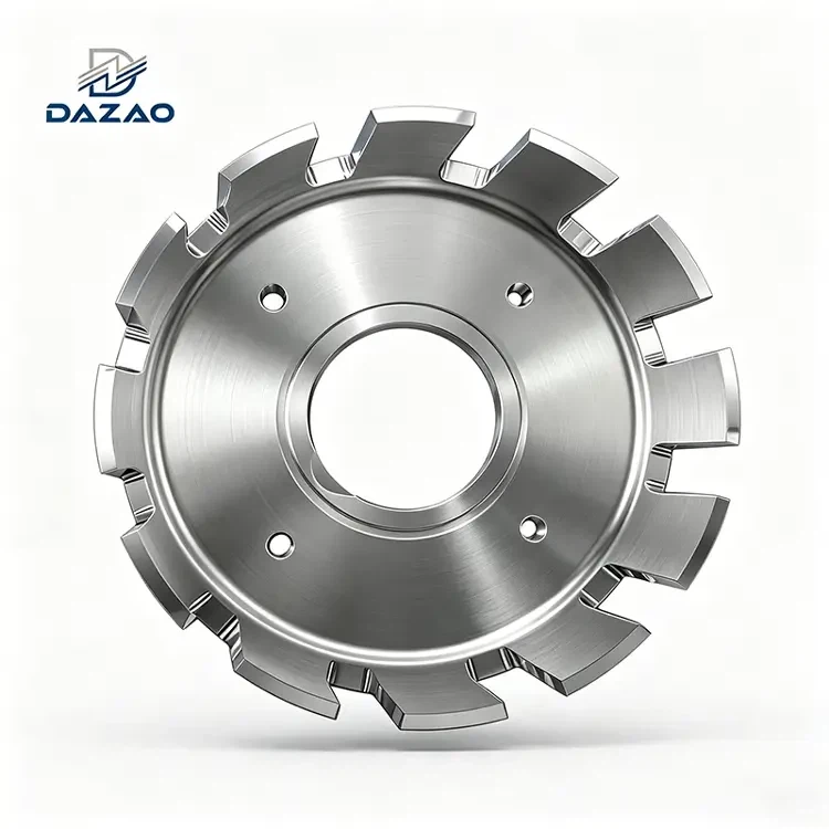
· Engineering Action: We introduced mirror milling using specialized face-milling cutter geometry followed by precision hand lapping. Surface flatness was brought within ≤0.02 mm/m and roughness was reduced to Ra 0.4 µm. Every precision machined stainless steel components run now undergoes 100% helium mass spectrometer testing prior to dispatch, elevating assembly acceptance rates to 100%.
2: Outgassing Mitigation in Spherical UHV Reaction Vessels
· Root Cause: A research institute reported base pressures stalling at 10^-7 Pa inside a spherical uhv chamber with cf flanges made from standard SS304. High outgassing rates from internal surface contamination and trapped moisture prevented pump-down to the required 10^-9 Pa level.
· Engineering Action: We changed the material specification to low-carbon SS316L, integrated a 900°C vacuum annealing degas cycle, and implemented internal electropolishing to lower surface roughness to Ra ≤ 0.2 µm. Following cleanroom ultrasonic washing and vacuum baking, ultimate vacuum reached 10^-9 Pa inside specification.
3: Load Lock Chamber Flange Warping Under Pressure Cycling
· Root Cause: A wafer equipment manufacturer detected progressive vacuum loss in a semiconductor load lock chamber design after six months of operation. Rapid vent-to-vacuum pressure cycling released residual machining stress, warping the main sealing door flange by 0.03 mm.
· Engineering Action: We instituted a two-stage stress relief process: rough milling → thermal annealing → semi-finishing → secondary thermal stabilization → 5-axis finish milling with tool-path micro-compensation. Post-modification load lock doors exhibited warp ≤0.01 mm after 10,000 pressure cycles.
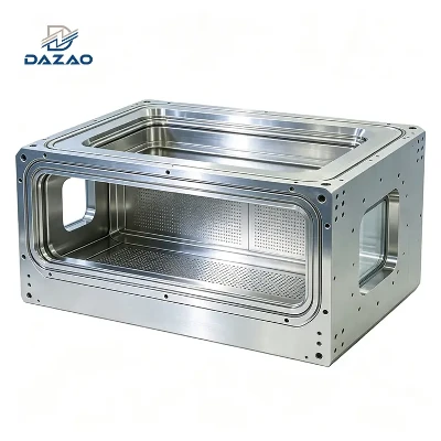
Technical Differentiators for Ultra-High Vacuum Fabrication
Standardized metallurgical and testing workflows that separate semiconductor-grade chambers from commercial machine shops.
1. Graded Vacuum Sealing & 100% Helium Leak Validation:
· High Vacuum (HV) Standard: Helium leak rate ≤1×10^-10 Pa·m³/s. Optimized for PVD systems, load locks, and transfer modules.
· Ultra-High Vacuum (UHV) Standard: Helium leak rate ≤1×10^-12 Pa·m³/s. Formulated for plasma etching and surface analysis systems.
2. UHV Material Outgassing Control Protocol:
· Material lot traceability with low vapor pressure alloy selection (SS316L, Al6061-T6).
· High-vacuum thermal degas processing removes absorbed hydrogen from internal metal lattices.
· Electropolishing reduces micro-porosity and surface absorption surface area.
3. Cyclic Load Stress Stabilization:
· Double-stage thermal annealing eliminates residual machining stresses.
· Toolpath compensation prevents structural deflection under atmospheric pressure loads.
Performance Comparison: Monoblock 5-Axis Milling vs. Welded Assemblies
Quantitative evaluation of vacuum integrity, precision, and long-term operating costs.
|
Evaluation Metric |
Monoblock 5-Axis CNC Milling |
Welded Sheet Metal Assembly |
Structural & Process Impact |
|
Vacuum Leak Risk |
Zero internal weld seams; solid billet geometry |
High risk at heat-affected zone (HAZ) weld lines |
Prevents fatigue cracking during continuous vacuum cycles |
|
Flange Flatness |
Flatness ≤0.02 mm/m; bores held to ±0.005 mm |
Thermal deformation distorts flatness beyond 0.10 mm |
Ensures precise wafer transfer robot arm alignment |
|
Outgassing Rate |
Low surface area; electropolished Ra ≤0.2 µm |
High outgassing from rough weld seams & flux inclusions |
Accelerates chamber pump-down to ultimate vacuum levels |
|
Internal Channels |
Monolithic fluid channels & complex ports |
External welded fluid lines & welded manifolds |
Prevents internal coolant leak paths inside vacuum boundaries |
|
Prototyping Lead Time |
Direct CAD-to-CNC milling without hard tooling |
Requires welding fixtures, press tools, and alignment jigs |
Reduces engineering iteration timelines for new tools |
For applications requiring optimized thermal management or corrosion barrier protection, our post-machining capabilities include certified hard coat anodizing and electropolishing options matching toolmaker standards.
Technical Specifications Table
Rigorous tolerances, surface finishes, and inspection standards for vacuum chambers.
|
Parameter Category |
High Vacuum (HV) Standard |
Ultra-High Vacuum (UHV) Standard |
|
Material Options |
SS304, Al6061-T6, Al7075-T6 |
SS316L (Low Carbon), Titanium Grade 2 |
|
Maximum Size Envelope |
1800 mm × 1500 mm × 800 mm |
1200 mm Spherical / Cylindrical Envelope |
|
Flange Flatness |
≤ 0.02 mm / m |
≤ 0.01 mm / m |
|
Machining Tolerances |
±0.010 mm |
±0.005 mm |
|
Surface Finish (Internal) |
Ra 0.8 µm (As-milled / Bead blasted) |
Ra 0.2 µm (Electropolished) |
|
Helium Leak Rate |
≤ 1×10^-10 Pa·m³/s |
≤ 1×10^-12 Pa·m³/s |
|
Base Operating Pressure |
Down to 10^-7 Pa |
Down to 10^-9 Pa |
|
Machining Equipment |
5-Axis Simultaneous Milling, Turn-Mill |
5-Axis Gantry Milling, Jig Grinding |
|
Quality Documentation |
CMM Inspection Report, Material Cert (EN 10204 3.1) |
Helium Leak Detector Logs, Outgassing Data |
Quality Assurance & Inspection Standards
Verification protocols ensuring direct integration into semiconductor fab lines.
Our manufacturing operations run under an ISO 9001:2015 certified quality management system. Inspection protocols cover every phase of chamber fabrication:
· Material Inspection: Incoming material lots undergo chemical verification via Optical Emission Spectroscopy (OES). Ultrasonic checks verify zero internal void formation in thick extrusions.
· First Article Inspection (FAI): FAI dimension reports are generated using Zeiss CMM equipment before releasing full batch production runs.
· In-Process Precision Checks: Critical sealing dimensions, O-ring groove geometry, and ConFlat (CF) knife-edge profiles are verified during milling operations.
· 100% Helium Leak Testing: Every box shaped high vacuum chamber undergoes leak verification using Pfeiffer Helium Mass Spectrometer Leak Detectors operating in vacuum mode.
· Cleanroom Packaging: Parts undergo ultrasonic cleaning with deionized water, vacuum bakeout degas, double polyethylene bagging in a cleanroom, and protective crating.
Material and Geometry Selection Matrix
Matching material properties and structural shapes to process gas environments and vacuum ranges.
· Stainless Steel 304 / 316L: Selected for operating bakeout temperatures >200°C, reactive process chemistry, and ultimate vacuum requirements below 10^-7 Pa. SS316L is specified for chlorine and fluorine plasma etching processes.
· Aluminum 6061-T6: Applied where thermal dissipation, reduced weight for robotic wafer handlers, and fast pump-down cycles are required. Aluminum oxide surface passivation provides an effective outgassing barrier.
· Box / Rectangular Enclosures: Delivers maximum internal substrate loading volume. Recommended for pvd deposition system vacuum chamber builds and automated transfer modules.
· Spherical / Cylindrical Enclosures: Distributes structural pressure stresses evenly under full atmospheric differential loads. Ideal for spherical uhv chamber with cf flanges operating in scientific and surface analysis fields.
Target Application Industries
Serving global semiconductor OEMs, coating equipment builders, and scientific research labs.
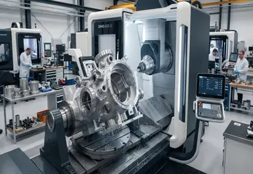
Semiconductor Wafer Processing
Production of plasma etching chamber semiconductor equipment, CVD enclosures, and ion beam modules.
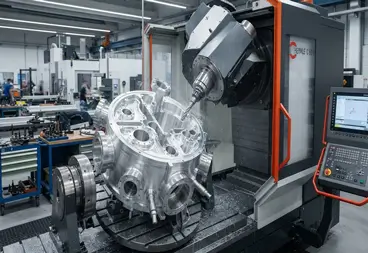
PVD Thin-Film Deposition
Monolithic chamber bodies with integrated target flanges and internal cooling for sputtering systems.
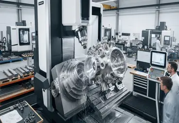
UHV Research Laboratories
Custom UHV chambers built for synchrotron light sources, surface physics, and particle acceleration systems.
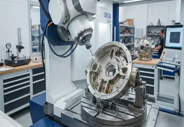
Tool Maintenance & Refurbishment
Re-machining and exact-fit replacement of precision CNC vacuum chamber components for legacy wafer fab lines.
FAQs
01.How do you distinguish between a real vacuum leak and material outgassing during testing?
02.Why select aluminum 6061-T6 over stainless steel for semiconductor vacuum chambers?
03.How do you prevent damage and burrs on ConFlat (CF) knife-edge flanges during 5-axis machining?
04.Why can a vacuum chamber pass static CMM inspection but fail helium leak testing?
05.What prevents load lock chamber flanges from warping during frequent pressure cycling?
06.How does internal surface roughness (Ra) affect vacuum base pressure?
Request a DFM Evaluation for Your Semiconductor Chamber Design
Submit your 2D engineering drawings and 3D CAD files (STEP, IGES, X_T) for an engineering assessment.
Our technical team delivers detailed Design for Manufacturability (DFM) feedback and formal commercial quotes within 24 hours.
Direct Technical Email: Erica@dazaocn.com
Contact Us

Hot Tags: 5 Axis CNC Machining Semiconductor Vacuum Chamber,ultra high vacuum chamber fabrication,semiconductor load lock chamber design,box shaped high vacuum chamber,spherical uhv chamber with cf flanges